


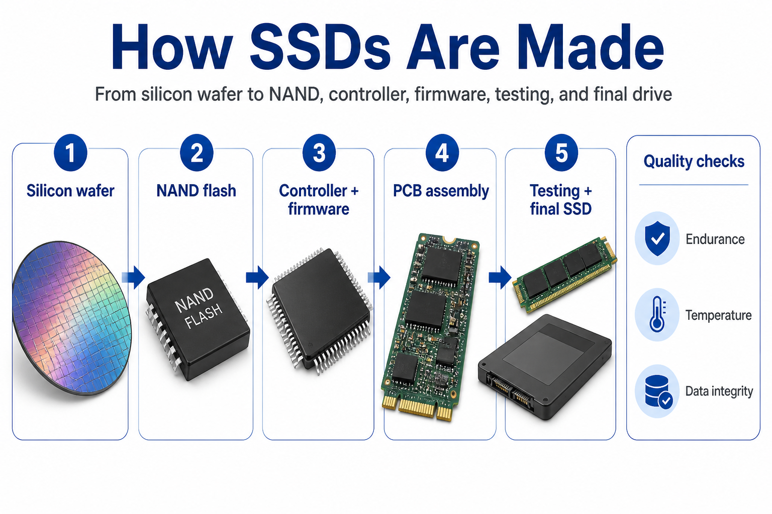
SSDs are made by combining NAND flash memory, a controller, firmware, a printed circuit board, connectors, and quality testing into a finished storage device. The process starts with silicon wafers and ends with a drive that must reliably store data under real workloads.
Quick Answer
- Core materials: silicon, NAND flash, controller silicon, PCB, connectors, and packaging materials.
- Main steps: wafer fabrication, NAND packaging, controller and firmware, PCB assembly, testing, and final drive preparation.
- Quality matters: endurance, temperature behavior, firmware stability, and data integrity separate serious SSDs from weak ones.
- Industrial SSDs add more checks: lifecycle control, operating range, and application fit become part of the manufacturing decision.
How SSDs Are Made: Step by Step
| Step | What Happens | Why It Matters |
|---|---|---|
| Silicon wafer | Semiconductor wafers are fabricated for NAND and controller chips. | This is the base of flash storage. |
| NAND flash | Memory dies are packaged and prepared for storage use. | NAND quality affects endurance and capacity. |
| Controller + firmware | The SSD controller manages reads, writes, wear leveling, and error handling. | Firmware determines much of the user experience. |
| PCB assembly | NAND, controller, power components, and connector are assembled. | Layout and components affect stability and compatibility. |
| Testing | Finished drives are checked for performance, errors, and reliability. | Testing reduces field-failure risk. |
Related guides: what TBW means, SSD power loss protection, and SSD reliability and data security.
Detailed Manufacturing Journey
⚡ Key Takeaways
- SSD manufacturing starts with ultra-pure silicon — refined from sand to 99.9999999% purity (nine nines).
- NAND flash chips are built layer by layer using photolithography, with modern 3D NAND stacking 200+ layers on a single die.
- Assembly involves bonding NAND dies, a controller chip, and (sometimes) DRAM onto a PCB — then enclosing it in the final form factor.
- Testing is where quality separates from junk. At Qootec, every drive goes through burn-in, thermal cycling, and full-surface verification before shipping.
- The entire process — from wafer to boxed product — involves 500+ individual steps across multiple facilities and countries.
📑 Table of Contents
People ask me this question all the time when they visit our Shenzhen facility: “How do you actually make these things?” They’re holding a tiny M.2 stick that weighs less than a house key, and they can’t quite believe it can store two terabytes of data and read it back at 7,000 megabytes per second.
The honest answer is: it’s complicated. Really complicated. The full journey from raw materials to a finished SSD involves hundreds of steps, nanometer-scale precision, and a global supply chain. But I’ll break it down into the major stages so you can appreciate what goes into every drive — and why quality control matters so much more than most people realize.
The Big Picture: Sand to SSD
Here’s the simplified pipeline:
- Silicon purification — Turn sand into ultra-pure silicon crystal
- NAND fabrication — Build billions of memory cells on silicon wafers using photolithography
- Wafer testing — Test every die, sort by quality grade
- Assembly — Mount NAND dies + controller + DRAM onto a PCB
- Firmware — Program the controller with the drive’s operating software
- Final testing — Burn-in, thermal cycling, performance verification
Steps 1–3 happen at semiconductor fabs (Samsung, SK Hynix, Micron, YMTC, etc.). Steps 4–6 happen at SSD manufacturers like us. Let me walk through each stage.
Stage 1: From Sand to Silicon Wafers
Every SSD begins its life as silicon dioxide — the main component of ordinary sand. But the silicon in your SSD is nothing like beach sand. It’s been refined to a purity of 99.9999999% — that’s “nine nines” purity, one of the purest materials humans produce.
The Czochralski Process
Purified silicon is melted in a crucible at 1,414°C. A small seed crystal is dipped into the molten silicon and slowly rotated and pulled upward over several hours. As it rises, silicon atoms attach to the seed in a perfect crystalline structure, forming a cylindrical ingot — typically 300mm (12 inches) in diameter and weighing over 100 kg.
This ingot is then sliced into wafers less than 1mm thick using diamond-wire saws. Each wafer is polished to an almost atomic-level smoothness — any imperfection at this stage would ruin thousands of chips downstream. These wafers are the “canvas” on which NAND flash memory will be built.
Stage 2: NAND Flash Fabrication
This is where the real magic happens — and where billions of dollars of R&D investment come into play. NAND fabrication uses photolithography to build microscopic memory cells on the silicon wafer, layer by layer.
How Photolithography Works
Think of it like printing a photograph, but at a scale thousands of times smaller than a human hair:
- Deposition: A thin layer of material (oxide, nitride, or polysilicon) is deposited on the wafer surface.
- Coating: A light-sensitive chemical called photoresist is applied on top.
- Exposure: Ultraviolet light is projected through a mask (like a stencil) onto the photoresist, transferring the circuit pattern.
- Etching: Chemical or plasma etching removes the unwanted material, leaving the desired pattern behind.
- Repeat: This cycle repeats dozens of times to build up the complete cell structure.
The 3D NAND Revolution
Here’s where modern SSDs get their massive capacity. Traditional planar (2D) NAND laid memory cells flat on the wafer surface — you could only fit so many before hitting physical limits. 3D NAND changed everything by stacking cells vertically, like building a skyscraper instead of a sprawling suburb.
Current-generation 3D NAND stacks 176-232 layers high. Samsung, Micron, and SK Hynix are pushing toward 300+ layers. Each layer adds capacity without increasing the wafer footprint. It’s an engineering marvel — imagine etching holes through a 200-layer stack with near-perfect precision, then filling those holes with conductive material to create vertical channels.
At our Shenzhen facility, we work with wafers from these major foundries. When a new batch arrives, we can literally see the technology evolution — newer wafers are thinner, denser, and pack exponentially more storage into the same physical space.
Stage 3: Wafer Testing and Sorting
Not every chip on a wafer is perfect. Microscopic defects, contamination, or process variations mean some cells will fail. Before cutting the wafer into individual dies, manufacturers test every single chip.
Automated probe stations make contact with test pads on each die, running electrical tests to verify:
- Memory cell functionality (can each cell store and retrieve data?)
- Write/erase cycle endurance
- Data retention capability
- Speed performance (read/write latency)
Dies are graded into bins based on performance. The best ones become high-end consumer or enterprise SSDs. Lower-grade dies might go into budget drives or get discarded entirely. This binning process is why you see such a wide range of SSD prices and performance tiers — they often come from the same wafer, just different quality zones.
Stage 4: Die Assembly and Packaging
Once tested, the wafer is diced into individual chips using precision saws. These tiny dies — often just 10-15mm on a side — are then assembled into the SSD you’ll eventually use.
PCB Assembly
The SSD’s printed circuit board (PCB) is populated with components:
- NAND flash dies: Multiple chips are mounted and wire-bonded or flip-chip bonded to the PCB
- Controller chip: The “brain” that manages data flow, wear leveling, and error correction
- DRAM cache: High-end SSDs include DDR4 chips for faster buffering
- Power management ICs: Regulate voltage and protect against power loss
This happens in cleanroom environments — even a speck of dust can cause connection failures. Automated pick-and-place machines position components with micron-level accuracy, then reflow soldering permanently attaches them.
Form Factor Packaging
The assembled PCB is fitted into its final form factor:
- 2.5″ SATA: Enclosed in a metal or plastic case, mimicking traditional HDD dimensions
- M.2: The bare PCB itself, designed to plug directly into motherboard slots
- U.2/U.3: Enterprise drives with hot-swap capabilities
- PCIe add-in cards: High-performance drives that look like graphics cards
We handle this final assembly stage in-house for many of our 2.5″ SATA SSDs and industrial M.2 modules. It gives us direct quality control over the finished product.
Stage 5: Firmware Programming and Initialization
An SSD without firmware is just a collection of silicon and circuits. The firmware is what makes it intelligent — handling wear leveling, garbage collection, error correction, and communication with the host system.
During manufacturing, each drive is programmed with:
- Base firmware: Core operating code from the controller manufacturer (Phison, Silicon Motion, Marvell, etc.)
- Custom tuning: Brand-specific optimizations for performance or endurance
- Bad block tables: Mapping out any defective cells found during testing
- Over-provisioning allocation: Reserving extra capacity for wear leveling
This is also where the drive’s identity is set — serial numbers, model names, and capacity labels are written to firmware. For our industrial clients, we can customize firmware parameters to prioritize endurance over speed, or vice versa, depending on the application.
Stage 6: Quality Assurance and Burn-In
Before any SSD leaves the factory, it undergoes rigorous testing. This isn’t just a quick power-on check — it’s days of stress testing to catch early failures.
Burn-In Testing
Drives are subjected to:
- Temperature cycling: Rapid heating and cooling to expose thermal stress defects
- Write/erase cycles: Thousands of cycles to verify endurance claims
- Power cycling: Repeated on/off cycles to test power management
- Data integrity checks: Writing known patterns and verifying bit-perfect readback
Consumer drives might get 24-48 hours of burn-in. Our industrial SSDs go through 72+ hours because they’re destined for mission-critical applications where failure isn’t an option.
Final Inspection
Each drive is visually inspected for physical defects, then its SMART data is logged. Drives that pass get labeled, packaged, and shipped. Those that fail are analyzed — if it’s a firmware issue, they might be reflashed and retested. Hardware failures get scrapped.
Inside Qootec’s Manufacturing Process
We don’t fabricate NAND wafers ourselves — that requires billion-dollar fabs that only a handful of companies operate. But we do handle everything from die procurement through final assembly and testing.
Here’s what happens when you order from us:
- Die sourcing: We purchase tested NAND dies and controller chips from tier-1 suppliers
- PCB design: Our engineering team designs custom PCBs optimized for specific use cases (industrial temperature ranges, enhanced power loss protection, etc.)
- Assembly: In our Shenzhen facility, automated lines populate PCBs with components
- Firmware customization: We tune firmware parameters based on your workload requirements
- Extended testing: Industrial drives get our enhanced burn-in protocol
- Quality certification: Every batch is logged with full traceability
This hybrid approach lets us offer the reliability of tier-1 NAND with the flexibility of custom solutions. Need an SSD that operates at -40°C? We can do that. Need firmware tuned for write-heavy database workloads? We’ve got you covered.
Frequently Asked Questions
Who actually makes the NAND chips in SSDs?
Only six companies in the world fabricate NAND flash: Samsung, SK Hynix, Micron, Kioxia (formerly Toshiba), Western Digital, and Intel (though Intel exited the NAND business in 2021). Everyone else — including major SSD brands — buys NAND from these suppliers and assembles it into finished drives.
How long does it take to manufacture an SSD from start to finish?
NAND wafer fabrication takes 6-8 weeks. Die testing, assembly, firmware programming, and burn-in add another 1-2 weeks. So from raw silicon to finished SSD, you’re looking at roughly 2-3 months. This is why SSD prices can be volatile — manufacturers can’t quickly ramp production to meet sudden demand spikes.
Why are some SSDs so much more expensive than others?
Several factors drive cost: NAND type (SLC costs 5-10x more than QLC), controller quality (enterprise controllers have better error correction), additional components (DRAM cache, power loss protection capacitors), and testing rigor. A $50 consumer SSD and a $500 enterprise SSD might use similar NAND, but the enterprise drive has far more robust engineering around it.
Can SSDs be recycled?
Yes, but it’s complex. The NAND chips contain valuable materials (silicon, rare earth elements), but they’re difficult to separate from the PCB and packaging. Most e-waste recyclers focus on recovering precious metals from the circuit boards. Some manufacturers have take-back programs, but SSD recycling isn’t as established as HDD recycling yet.
The Bottom Line
SSD manufacturing is a fascinating blend of cutting-edge semiconductor fabrication and precision assembly. From growing silicon crystals to stacking 200+ layers of memory cells, every step requires extreme precision and quality control.
Understanding this process helps explain why SSDs cost what they do, why some drives are more reliable than others, and why capacity keeps growing while prices keep falling. It’s not magic — it’s relentless engineering innovation.
Need SSDs built to your exact specifications? Contact our team — we’ll walk you through the options and find the right solution for your application.

Shenzhen, China · Est. 2014
We’re a team of SSD and DRAM specialists with 10+ years in industrial storage. Got questions? Reach out — we’re happy to help.
Frequently Asked Questions
Where are most SSDs manufactured?
The majority of NAND flash production happens in South Korea (Samsung, SK Hynix), Japan (Kioxia), and the United States (Micron). However, final assembly often occurs in China, Taiwan, and Southeast Asia where labor costs are lower and supply chains are well-established. At Qootec, we source wafers globally but handle assembly and QA in our Shenzhen facility.
How long does it take to manufacture an SSD?
From raw silicon to finished drive, the process takes 2-3 months. Wafer fabrication alone requires 6-8 weeks due to the hundreds of photolithography steps. Assembly, firmware programming, and burn-in testing add another 2-4 weeks. Rush orders can be expedited, but quality testing shouldn’t be compromised.
Why are some SSDs so much more expensive than others?
Several factors drive cost: NAND type (SLC costs 5-10x more than QLC), controller quality (enterprise controllers have better error correction), binning (top-tier dies command premium prices), and testing rigor (industrial drives undergo longer burn-in). You’re not just paying for capacity — you’re paying for reliability and performance guarantees.
Can SSDs be recycled?
Yes, but it’s complex. The PCB contains valuable metals (gold, copper, palladium) that can be recovered. However, NAND flash chips themselves are difficult to recycle due to the complex layered structure. Most recycling focuses on component recovery rather than material reprocessing. We work with certified e-waste partners to ensure responsible disposal of failed units.
What’s the difference between consumer and industrial SSD manufacturing?
Industrial SSDs use higher-grade NAND (often SLC or MLC instead of TLC/QLC), undergo longer burn-in testing (72+ hours vs 24-48 hours), and include additional components like power-loss protection capacitors. The manufacturing process is fundamentally the same, but quality standards are stricter. Check our industrial SSD lineup to see the difference in specifications.
The Bottom Line
SSD manufacturing is one of the most technologically advanced processes in modern electronics. From growing perfect silicon crystals to stacking 200+ layers of memory cells with nanometer precision, every step requires extreme control and expertise.
Understanding how SSDs are made helps explain why quality varies so much between brands — and why cutting corners in manufacturing leads to reliability problems down the road. When you’re choosing an SSD, you’re not just buying storage capacity. You’re buying the accumulated expertise of engineers who’ve spent decades perfecting this process.
Need help selecting the right SSD for your application? Contact our team — we’ll walk you through the options and explain exactly what you’re getting at each price point.
Shenzhen, China · Est. 2014
We’re a team of SSD and DRAM specialists with 10+ years in industrial storage. Got questions? Reach out — we’re happy to help.